Pin assignments: Print and scribble all over the diagram
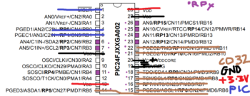
Here's the PIC24FJ64GA004 family pinout once again:
• Brown pins are 5V tolerant. We need seven for the CD32 and there's seven, so they're all spoken for.
• Red pins are +3.3V.
• Black pins are ground, and the tant cap.
• Blue pins are reset and ICSP.
The remaining vacant pins are 2-3, 6-7, 9-10-11-12 and 23-24-25-26. Of which 6-7, 11 and 23-24-25-26 are capable of SPI. It's a rotten shame that there's only three on the left side, since I need four for SPI SSELECT, MISO, MOSI and CLOCK. The PS2 ATTENTION pin doesn't need to be RPx, but I guess it would be neater.
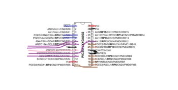
There's nothing stopping me from using one of the unused RPx pins from the other side of the chip over with a trace running under the chip in a Shenzhen I/O-style maneouver, like this:
I'm running it through pin 10 here, which would be set to idle at high-Z, since I'm not sure how precise the traces can be with these (assuming?) cheap boards. This seems to waste the least space and be the closest to my concept. The top right group of three pins could be something RPx-ish, or the 3-circuit DIP again.
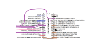
Alternatively, I could be silly and do this:
No thanks. Plus, shouldn't all the lines used in a bus be similar lengths?
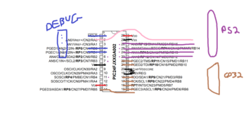
If I wanted to, I could take those four grouped RPx in the top right as a sign that I should put the PS2 interface on the right-hand side as well.
But that's a bit cramped I reckon. I was planning on having a series of large solder pads running down each side of the board, with large, easy-to-manage spacing. Having up to eighteen leads all on one side of the board is pushing it.
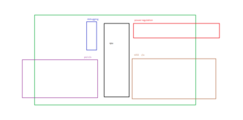
I'd rather have it all neatly spaced out like this.
And, yes, that looks just like the Ocelot diagram again. Simple works.
PUT OCELOT BLOCK DIAGRAM UP WHERE IM DESIGNING THE BOARD.
Super nice and neat and tidy. Only had to draw the same diagram six times. I bet that's a new low record somewhere...
Since the PIC requires a power supply pair in the lower left, I can also use it to power the PS2 pad, if I protect the pad and the PIC with caps. The presence of +V down there also lets me use it for the pull-ups required on the controller --> PIC MISO and ATTENTION lines.
On the CD32 side, the pull-ups are placed within the current-limiting resistors for the output-only UP, DOWN, LEFT, RIGHT, FIRE2OUT/DATAOUT lines. For the bidirectional/input-only JOYMODE/FRAME and FIRE1OUT/CLOCKIN lines, the pull-ups are placed outside the current-limiting resistors to allow the CD32 more control over the line.
There are no pull-ups on the DIP switches since the PIC has an internal weak pull-up capability for the purpose.
