I don't know why Autodesk wanted me to make an account first. It's creepy and unnecessary. Don't do that, Autodesk.
Here we go. This looks pretty awesome, I think!
EAGLE was actually pretty painless. Sure, the selection tools took a
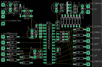
lot of getting used to, but I got there in the end. There's built in packages for tons of different devices, including the Microchip range, with all the pins labelled, etc. The default schematic pin spacing of the 28-pin PIC device was way too close together for a nice schematic (which is, I assume, why the CD32 schematic earlier had all sorts of ugly Z shapes in it when it could have been much more linear), so I had to duplicate and modify the footprint for it, which didn't take too long surprisingly.
Selecting resistor and capacitor footprints took a little while. There's no point making a board if the components don't fit in it, and there's no point getting components if I'd have to twist them six ways from Sunday to fit them into a board. Things like the tactile switch (which I will never stop instinctively trying to spell as 'tactical' for some reason) having four electrical contacts, for example. The X shapes for the interface connections are an EAGLE
THROUGH-HOLE PAD 3,17/1,3 (Version 1) from the
wirepad library. These will be large circular solder pads on the final PCB. I'm including a solder pad for the
NOT CONNECTED pin of the PS2, in case my extension lead has a wire for that pin. It doesn't have any traces to anything on the board, but it'll help anchor the lead in place. The reason I'm using a row of resistors for the pull-ups on the CD32 side is that at 6p per resistor, they're much cheaper than the cheapest resistor array I could find.
Resistor sizes are pointlessly obtuse. All I wanted to know was which one was the 'normal' size. Based on the following advice I found on a forum, which puts it as plainly as could be, I chose 0207/10 resistor footprint, which I believe are the standard rice-grain kind of sized ones.
• 0204 are those small (typical 1/8 W) resistors, about 5 by 1.5 mm.
• 0207 is the standard size for 1/4 W, about 6.5 by 2.5 mm.
• 0309 and 0411 are the next larger sizes.
(endquote)™
At this point I was simultaneously shopping for components on element14. Wait, Farnell. Wait, I was right the first time. Farnell is a tricky-ass company. There's like three different brands (at least), one is for industry, one is for consumer, and one is for export I think. They used to have very differently named sites, but they bought one, and then someone else bought them, and now they're all Farnell.
I think CPC Farnell is for consumers. They have less range, but they have some bulk pack discounts at the cost of buying unbranded products in packs instead of more traceable components in singles. Farnell (aka Element 14) is for industry. They have more range, and you can buy certain things singly, but they cost a little more. Except element14 was always 'the' Raspberry PI supplier for the UK, so I don't know. I could have saved a quid or two if I used CPC and even ended up with some leftover stuff. But I had a Farnell Farnell account for my ocelot so I used that this time. Some of the catalogue codes are the same between sites (or rather if you search for a Farnell code on CPC you get the CPC page for that same component with the CPC code). It is confus.
Speaking of resistors, here's today's "Most Useful Caption Award" winner:
'Dimensions are in millimetres and inches unless otherwise stated'. What does that
mean?
There's no weird dangling wires, and everything seems neat. You have to go back and make sure there's no wires that are simply overlapping rather than being correctly connected or vice-versa.
It is a very good idea to correctly name all the terminals and inputs and devices you're placing, and then use the ERC Errors tool to help you find any inconsistencies or dangerous connections. Here, it's telling me that the capacitors along the bottom left are very close to the horizontal lines running out to the PS2
ACKNOWLEDGE and
DATA inputs. The
POWER warnings are telling me that I've connected pins designated as power pins in the PIC device to places in the schematic - I assume it would be happier if I used one of those ghostly
Vcc and
GND connections with the symbols just floating off in space instead of explicitly wiring them to the regulator.

Now I have to put things down on the board in a way that makes sense, and then route them together with ideally direct traces that minimize reflections and losses. Luckily for me, I've been preparing for this day my whole life - I've played every Amiga puzzle game under the sun.
I already had a go of laying this out physically in that wiggly-line sketch a short while back. One component that I've removed between then and now is an electrolytic capacitor at the top right of the PIC. My novice-but-safe approach was to have an electrolytic-ceramic pair together wherever I needed power stability - so whenever a power supply pair enters or leaves the board, either side of the regulator, and on each power pin pair on the PIC. I've removed the electrolytic at the top right of the PIC since it's very close to the electrolytic on the regulator, so there's no reason to duplicate it.
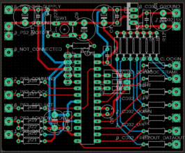
The yellow lines indicate connections that have to be routed somehow. There's an automatic router, but it makes a bit of a mess of the situation, and I think I can do it a bit better with my conceptual knowledge of the intended design of the board. Although I'm pretty sure this interpretation isn't strictly true, I still think of the current hitting each component in a linear order, so I want my super-stable post-filtering power supply rails to be connected to the regulator first, with everything requiring power from it to be connected afterwards. EAGLE's automatic router just sees all the components connected to a single node and draws lines however it likes - like trying to connect the +5V pull-up resistors directly to the solder pads in the top right instead of after the board-input power filtering stage.

Zero vias! I'm using the posts of the components as ways to swap signals from being on the top or bottom layers of the board.
Notice how I'm using different trace thicknesses for the power and signal traces. This is done using classes. Make a note!
I'm not entirely sold on the way the traces for
CD32_FIRE2OUT_CLOCKIN and
CD32_JOYMODE_FRAME slide in sneakily through the connections of the DIP switch, but if EAGLE says it's okay, it's okay. I guess I'm going to be testing the capability of those PCB manufacturers after all. This does mean that the sneaky wire that goes underneath the PIC might not be entirely necessary since it could have gone around pin 9 on the PIC, but there's no pressing reason to free that pin, so I'm going to stick with the plan.
If you're wondering why I don't have a ground plane, it's because I don't know what one is or what it's for. Well, I do, but not to a great enough extent that I'm willing to bet money on it.
Phew. It's done. I could get this made now! But... I need a cool logo! There's a big blank space on the board there next to the
PS2_8_NOT_CONNECTED pin...