PSCD32 Development Diary

Good morning, PSCD32!

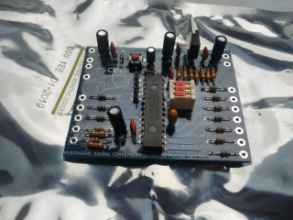
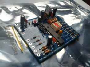
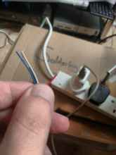
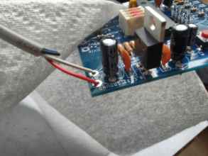
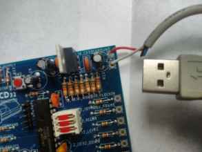
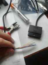
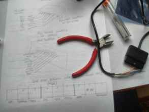
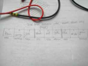
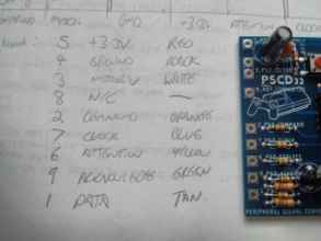
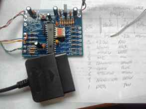
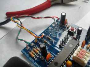
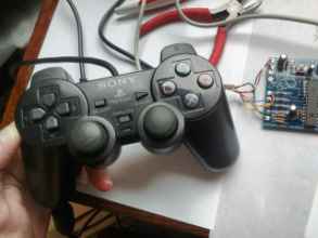
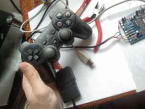
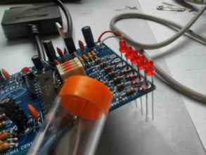
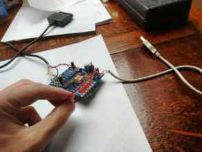
Where were we? Oh wow, yeah, this thing! It's real! How cool is that? But now I have to make it do something other than just look amazing... Here's my plan: • I'm going to solder on five LEDs to the Up, Down, Left, Right and Fire2Out unidirectional outputs of the CD32 side so I can temporarily use them as indicator lights while I get the PS2 side to work. I could leave the pad until later and have them as lights by themselves, but I'm confident enough to skip the 'just get a light blinking with nothing else at all soldered on' stage (I'm still going to do it, just with the pad available). • I'm going to power the pad from a mains USB +5V power supply. This is going to be my substitute for the CD32's power supply. I don't have a bench power supply. I'm using what claims to be an Apple-branded charger, so I hope it'll be stable. It'll surely be nicer than the CD32's twenty-five year old electronics... • To get the USB power into the board, I'm going to chop up a USB A cable and solder the +5V and ground leads onto the board, and have a male A lead ready to plug into the charger. • On the left side, I'm going to split, strip and solder the Playstation extension cable to the nine terminals on the board. Here we go. Cutting and stripping leads is easy if you're careful. You should probably tin leads before you solder them in place, but I don't always do that. These big holes I laid down are perfect for this job. You might notice that I'm not soldering the correct leads into the correct locations according to the colours given in the USB specification. This is because this is a Wire of Lies. You can only trust reality - use your multimeter in continuity to determine which leads go to which terminals on the USB plug side, and then confirm this by using a voltage test against the exposed leads when the power has been applied. ... you should probably wear gloves for that last part if your charger isn't very trustworthy. With the ability to apply power to the board, you can test a lot more now: you can test if the pull-up resistors are installed correctly, and whether the regulator is providing power to the PIC properly. If you had a signal analyser, you could possibly see the MCU's default internal Fast RC oscillator being fired out of its butt at the CLKO pin, pin 10. I don't know why by default the PIC clock is set to output on that pin, but it is, and it's confusing if you don't know how to turn it off and use it as GPIO. I have gotten this wrong before - Murphy says that any component that can fit equally well turned 180 degrees probably should be turned 180 degrees. But I've stared at the Micrel datasheet for hours and I'm sure I got it right. With the Ocelot, I made a mistake with a tiny, transistor-package-like regulator, and had to cut it out and rearrange the power section to accomodate a better regulator installed correctly. Next up, stripping the Playstation extension cable. First, you should use it with a real Playstation to test if it works! Here's my cut and stripped cable. I've got eight leads, as expected. The NOT CONNECTED lead isn't present. Now I'm going to test each pin in turn to see which colour lead it goes to. Drawing lots of clear diagrams at this point is essential. You could really blow something up if you get it the wrong way around. Other people's tutorials may give you the colours to use, but as with the USB cable, everything is totally arbitrary. Even official controllers won't have the same colours for the same leads every time, I'd bet. You Have To Test. And there we go. Double check to make sure. Write down the colours you get, and list them in the order that they should appear on the board. I've decided to twist the wires together into pairs or braid them into triads before soldering them to the board. Not for signal reasons, but just because it looks nicer, and maybe it's physically stronger? Because you haven't been a buffoon and mutilated and soldered a real Playstation pad to the board instead of an extension cable, you can use the end of the cable to test continuity - put one probe on a safety pin inserted into a hole in the socket you've attached to the PSCD32, and the other probe onto the appropriate location on the board. If you can identify the correct path from the ATTENTION pin on the socket to the corresponding pin on the PIC with the correct resistance being reported by the multimeter, everything is cool! You should also be able to see +3.3V on the supply pin in the socket when you apply power to the board. That means that if you were to attach a controller, it would work... That's it! What I have now is a device, powered by USB +5V power, with a PS2 controller socket. Plug in the USB power, turn it on. Then press the Analog button on the controller... if it lights up, the pad is being powered correctly! The default behaviour of the pad is to be in Digital mode when it powers up, so don't be surprised if the light doesn't come on by itself. Also, this means that if there's a break in one of the leads somewhere and the power is interrupted, the Analog light will go out. If it doesn't go out when you wiggle the controller a little, the leads are good and everything is shiny. This post is not sponsored by Sony, btw. If they didn't want their name on pictures of items they manufacture, they shouldn't print their name on items they manufacture. Right, let's unplug that for now, since I don't need the pad attached to test the board and the PICkit behaviour. Here's my array of LEDs, reporting for duty. I've soldered the negative terminals to the CD32 interface pads. The positive leads need to be all soldered together and linked to either the +3.3V or +5V rails. This creates a sequence of (+5V)--->|---(470R)---(PIC GPIO), so I can toggle the LED on and off by setting the GPIO to open-drain low or high-Z. The soldering work down there isn't pretty, but it's functional. And that's all the hardware work that's needed. It's time to plug this thing into my PC, and see how much damage it does. I've got my PICkit 2, I've got my charger, I've got my anti-static bag for the device to rest on, I've got a Playstation 2 pad. Let's see what happens! Aw yeah! This is a Timer incrementing a variable at regular intervals and setting five bits of PORTB to that value. There's also a whole bunch of other stuff involved to get this far: connecting the PICkit 2 to MPLAB X, starting a project, getting it to compile, setting the directionality of the pins, enabling/disabling remappable peripheral modules of the PIC, setting the clock speed. This means: • The PICkit hasn't blown up. • My PC hasn't blown up. • The USB power supply is working. • The PICkit ICSP header is installed nicely. • I inserted the ribbon connector between the PICkit and the board the right way around. • The PICkit is communicating with the PIC correctly. • The LEDs are the right way around. • The LEDs, the resistors, and all the other components are somewhat-appropriate values. • The PIC itself and all its capacitors are installed and working. • I still know how to write code that increments a variable. This is good news all round! The next easiest thing is to have it read the state of the DIP switches so I can interact with the gizmo somewhat in real-time. To do that, I activate the Change Notification Pull-ups, which act as weak pull-ups within the specified pins within the PIC. These let you attach switches or keypads to the PIC directly without having to supply external pull-up resistors. The open or closed state of the switches can be read by reading the voltage at the pin through PORTx. I mounted my DIP switches so that the open state was left and the closed state was right, purely because that matched the numbers 1, 2 and 3 on the component I bought. A few abstractions later, and I can interrogate the switches with DIP_SWITCH_1_IS_RIGHT() macros and twiddle the lights manually. Yay! All that's left is to work out how to communicate with the PS2 pad.
Easy as SPI

First, tutorials which teach you how to interface with a PS2 controller through Arduino are more or less useless. • I'm going to qualify the above comment with some context. The tutorials which tell you to use a library are useless if you want to write your own library and get things working (or, obviously, if you don't have an Arduino :) ). There's a lot of value in being able to use someone else's library if you want to prototype things quickly, or you're unsure about electronics and you'd like some reassurance that 'useful things' are within your grasp. Also, you can open the source for the library if you're a sneaky cheater... or just stuck. Free software is free software for a reason. :) • Also, you still have to figure out how to get the controller physically linked to the Arduino board, which is simple but not trivial. Here's the resources I have for the PS2 protocol: • Curiousinventors PS2 interfacing page http://store.curiousinventor.com/PS2McCubbin's site https://gamesx.com/controldata/psxcont/psxcont.htmScanlime's github gist https://gist.github.com/scanlime/5042071Everything You Have Always Wanted to Know about the Playstation But Were Afraid To Ask by Joshua Walker. http://hitmen.c02.at/files/docs/psx/psx.pdfpinouts.ru https://pinouts.ru/Game/playstation_9_pinout.shtmlNear Future Laboratory - PlayStation 2 Logic Analysis http://blog.nearfuturelaboratory.com/2008/06/19/playstation2-logic-analysis/ In the Playstation controller protocol, SPI (or a protocol compatible with it) is used to exchange 8-bit messages with the controller. The protocol uses all four SPI pins, with an additional fifth: • SSELECT pad <- PS2, a signal used to identify the target of a SPI communication, this is usually called ATTENTION in PS1/2 reverse engineering docs. • CLOCK pad <- PS2. • MOSI pad <- PS2, Master-Out-Slave-In, also known as COMMAND. In this case, I'm designating the PSCD32 as the Master and the PS2 controller as the Slave. • MISO pad -> PS2, Master-In-Slave-Out, also known as DATA. • ACKNOWLEDGE pad -> PS2. It is strobed negative after each byte has been sent by the controller except the final, which seems to me to indicate 'at least one more byte left in my response to your request', though none of the material I've found has made that suggestion. The protocol is simultaneous duplex, controlled and clocked by the console, or, in this case, the PSCD32 imitating the console. • A message exchange begins by the PSCD32 pulling ATTENTION low. • The CLOCK signal is pulled low by the PSCD32 as it puts the least significant bit of COMMAND on the bus. The controller simultaneously does the same with the least significant bit of DATA. • The CLOCK signal rises, and both devices sample their data lines. The clock frequency is in the range 100-250Khz (cycles, not switch events) according what I've read. • Eight bits are transmitted total, with the clock remaining idle high after the transmission. • If the pad has additional bytes to send, it strobes the ACKNOWLEDGE line low. The PIC24 family has hardware modules for performing SPI in hardware outside of the main CPU execution, which is just the ticket for this project. When triggered, it exchanges a single byte with the connected hardware, and can fire an interrupt. On the Ocelot, this is used together with DMA to continuously send data at high speed, but I don't need to do that in this scenario. What I want to do is set up the following sequence: • On PIC start-up, pins 6, 7, 26 and 11 are assigned to the SPI1 module, pins 9 and 10 are set to input. The parameters of the SPI such as clock edges are input to the module. • A timer interrupt triggers on a regular frequency greater than 60Hz. The objective of this event is to poll the pad through SPI and place the current controller state into memory: all the buttons and the analogue sticks. The greater the frequency, the more responsive the pad will feel. Amiga/Atari joysticks contain nothing but switches, so their state is updated instanteously and constantly. This is the behaviour I'm trying to emulate. The Amiga hardware allows its software to sense the states of its directional and fire joystick pins at any time, so there is no polling from the Amiga system to respond to. • The interrupt initialises a structure that abstracts a PS2-PSCD32 exchange: it holds the number of bytes to transmit, and arrays containing transmitted and received data. • The SPI module is instructed to send the first byte of the message. When the byte duplex transfer is complete, a SPI Transmission Complete Interrupt will fire. • The SPI transmission complete interrupt is used to store the received byte from the buffer, update the state of the exchange structure, and send the next byte if there is one. Otherwise, a function to analyse the received message is called. • The received message function unpacks the pad controller state from the message response into memory. • With the controller state unpacked, I can set the state of the CD32-side output pins to toggle the LEDs on and off. Since the Up, Down, Left and Right outputs will be simple open-drain Lows on the final device, if I can get it working with the LEDs, then that will be the directional part of the device done already! • I'm going to ignore the ACKNOWLEDGE line for now since I control the length of the exchanges and know the correct length they should be. I'll assume that making ATTENTION high aborts the current communication, and making it low starts a new empty one so I don't need to worry about left-over bytes (if there are any). MENTION THE DESIGN OF THE ELECTRONICS WHY I NEED PULL UP RESISTORS AND WHERE AND STUFF ON CD32 SIDE. A typical exchange with an original PS1 digital controller or an analogue controller in digital mode looks like this:
Playstation0x010x420xFF0xFF0xFF
Controller0xFF0x410x5Adatadata
The message is defined as being five bytes long (pending any further configuration by the Playstation side - it's possible to request a longer response to poll the pressure sensitive buttons). • 0x01 is an attention message to begin an exchange. The controller idles its response data line which is read as 0xFF. • 0x42 polls the controller for its button state. Meanwhile the controller responds to 0x01 with 0x41 indicating its controller type and data length in 16-bit words. • 0x00 0x00 0x00 from the Playstation are dummy messages to allow the controller to respond to the request. • 0x5A is a spacer message used when the controller is not ready to respond yet. • The controller responds to 0x42 with two data messages holding the button state response bitfields. Download all the docs for your chip. You've got the Datasheet, the C Programmers Guide, the Programmers Reference and the Errata. On top of that, Microchip separates out generic 'Reference Manuals' documentation common to PIC family MCUs into a series of a few dozen standalone chapters ('SPI', 'Timers', 'Interrupts', etc.) that have to be downloaded separately. Microchip's website has a single button that'll give you a .zip file with all the chapters combined together, if you can find it. Get the 'Application Notes' too. Unfortunately, they don't title these files with anything other than their internal reference number, so you'll have to manually read each one and rename them to their useful name. Or use DownThemAll! sneakily to automatically rename the downloaded files to match their textual link names. Cross reference all the documents against one another. Bitfields and structures are given different names in different documentation, and their descriptions will often differ slightly. The independent module chapters often contain example code to get you started transmitting with SPI. Go slow, use your debugger. That is why you spent money on a fancy PICkit, right? Too bad I didn't equip this with an LCD screen so I can see what it's thinking.

Treachery in SPIcraft

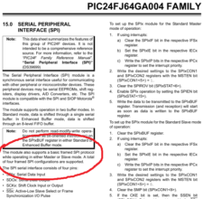
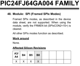
It didn't work. In fact, it doubly didn't work. No matter what combination of polarities and messages I attempted to send to the PS2 pad, I didn't get any responses that made sense. I was looking for the 0x5A spacer in the response, and couldn't see anything but 0xFF. The errata document for a chip details all the features or documentation that were mis-specified, omitted, incorrectly implemented, skipped, or just plain buggered somewhere between conception and production. On an idle whim, I found myself reading through the errata for the chip, front to back, and I found this particular gem. A whole feature described in detail in the datasheet that, in fact, doesn't exist. I wonder how that happened? "An errata sheet, describing minor operational differences from the data sheet and recommended workarounds, may exist for current devices." I was quite frustrated to find this out. I was kind of going to rely on Framed SPI. Framed SPI is a mode of the SPI module which allows it to control the SELECT / ATTENTION line automatically during transfers. I use it in the Ocelot, and ordered the dsPIC33 specifically to match the protocol used in the TLV5618A DAC. What a bother. Ah well, I've soldered the microcontroller to the board now. I might as well give it a go using my backup plan! Bit-banging!